 WhatsApp: +86 16626708626
 Email:
  Phone: +86 16626708626
Description
Key Technical Specifications
| Parameter | Value |
|---|---|
| Manufacturer | ASYST |
| Part Number | 1380-101545-11 |
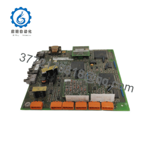
| Product Type | SMIF Indexer Connection PCB |
| Application | Semiconductor wafer handling |
| Equipment Function | SMIF indexer signal interconnection |
| Signal Type | Multi-channel digital I/O |
| Primary Function | Signal routing and distribution |
| Interface | Multi-pin harness / board connectors |
| Status Indication | On-board LED indicators |
| PCB Material | FR-4 |
| Mounting | Equipment-frame / bracket mounted PCB |
| Typical Environment | Semiconductor manufacturing equipment |
| Handling Requirement | ESD protection required |
| Weight | Approximately 0.15 kg reported by one secondary-market listing |
| Lifecycle | Legacy / limited aftermarket availability |
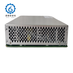
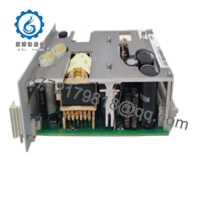
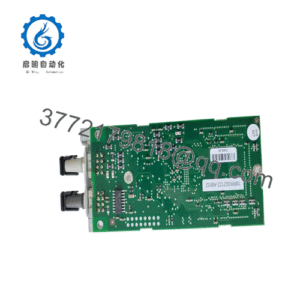
The available documentation describes the board as a passive signal-distribution/interconnection PCB for a SMIF indexer mechanism, routing signals between sensors, actuators, and the equipment controller. It also identifies multiple connector groups and onboard status LEDs.
A current secondary-market listing identifies the brand as ASYST, part number 1380-101545-11, and reports approximately 0.15 kg unit weight.
Important: Exact connector pin assignments, electrical ratings, and I/O channel counts should be verified from the equipment-specific schematic or board drawing. I would not substitute generic voltage/current values for those parameters without OEM documentation.
Product Introduction
The ASYST 1380-101545-11 is a SMIF indexer connection PCB used in semiconductor wafer-handling equipment. Its primary role is signal interconnection between the indexer mechanism, sensors, actuators, and the equipment control system. Available listings identify it specifically as an ASYST PCB, SMIF INDEXER CONN BOARD.
This is a machine-specific interconnect board rather than a general-purpose PLC I/O module. Replacement work therefore depends heavily on matching the original board revision, connector arrangement, cable harness, and machine configuration. Treat the exact part number as the primary purchasing identifier.
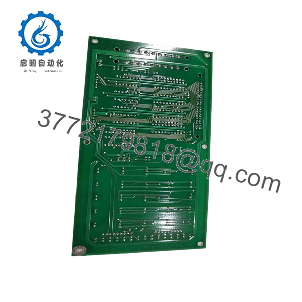
1380-101545-11
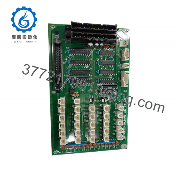
1380-101545-11
Installation & Configuration Guide
Stage 1: Pre-Installation Preparation — About 10 minutes
⚠️ Safety First: Place the semiconductor tool in its approved maintenance state. Follow the equipment manufacturer’s shutdown and LOTO procedure before opening the enclosure. Protect the board and exposed connectors from ESD and clean-room contamination.
Tools Required:
- ESD wrist strap
- ESD-safe work surface
- Phillips screwdriver
- Digital multimeter
- Cable labels
- Smartphone/camera
- Equipment electrical schematic
Data Backup:
- Confirm the installed board marking is 1380-101545-11.
- Photograph the entire PCB before touching the harness.
- Photograph every connector from multiple angles.
- Record connector and cable positions.
- Record all visible LED states.
- Obtain the applicable ASYST/TEL equipment schematic.
- Record any active indexer or wafer-handling alarms.
- Keep the removed board until the replacement has completed functional testing.
❗ This board is part of a machine-specific wiring architecture. Do not disconnect cables based on connector appearance alone.
Stage 2: Removing the Old PCB — About 5–10 minutes
- Shut down the wafer-handling equipment according to the OEM procedure.
- Isolate power where required.
- Verify the relevant supply is de-energized.
- Apply ESD protection.
- Photograph the board and all connected harnesses.
- Label each harness before removal.
- Disconnect connectors using their locking mechanisms.
- Do not pull on individual wires.
- Remove PCB mounting screws or retaining hardware.
- Lift the board away from the equipment frame.
- Inspect the harness connectors for bent contacts, contamination, or damaged locks.
⚠️ Semiconductor equipment harnesses can be tightly routed. Do not bend or twist them simply to gain access to the PCB.
Stage 3: Installing the New PCB — About 5–10 minutes
- Verify the replacement label reads ASYST 1380-101545-11.
- Compare the replacement PCB against the original board.
- Confirm connector count and physical locations.
- Inspect PCB contacts and connectors.
- Position the board in the original mounting location.
- Install and secure the mounting hardware.
- Reconnect each harness according to the photographs and schematic.
- Confirm every connector locking mechanism is fully engaged.
- Verify that no harness is under mechanical tension.
Configuration Clone — Critical:
This PCB generally does not function like a programmable PLC module with user-configurable firmware. The critical configuration is the physical wiring and machine-specific signal mapping.
Verify:
- Connector position
- Cable orientation
- Sensor wiring
- Actuator wiring
- Ground/reference connections
- LED channel correspondence
- Harness routing
Self-Checklist:
- Exact part number verified
- PCB revision compared
- All connectors matched
- Harness locks engaged
- PCB mounting secured
- No cables pinched
- ESD precautions maintained
Stage 4: Power-On & Functional Testing — About 10–20 minutes
- Perform a visual inspection before restoring power.
- Check for obvious shorts or damaged connectors.
- Restore equipment power according to the OEM procedure.
- Observe the PCB status LEDs.
- Check the equipment controller for new I/O faults.
- Exercise the indexer through the approved maintenance mode.
- Verify position sensors change state correctly.
- Verify actuator commands reach the appropriate devices.
- Run a controlled indexer cycle.
- Confirm the wafer/SMIF handling sequence completes without new alarms.
⚠️ Do not start with a full automatic wafer-transfer sequence. First prove the individual sensor and actuator signals in maintenance mode.
Technical Pitfall & Survival Guide
❗ 1. Connector Position Errors
This is the classic replacement mistake. A harness can physically fit a connector while being connected to the wrong board position.
Photograph every connector before removal. Then compare the replacement one connection at a time.
❗ 2. Damaged Connector Pins
A bent pin can produce an intermittent sensor or actuator fault that looks like a controller problem.
Inspect both the PCB connector and harness connector before power-up.
❗ 3. Wrong Board Revision
A matching base number does not necessarily guarantee identical electrical routing. Compare visible revision markings and PCB artwork before installation.
❗ 4. ESD Damage
This is a semiconductor-tool spare. Handle the board as an ESD-sensitive assembly even if it contains primarily passive signal-routing circuitry.
Use a grounded wrist strap and an ESD-safe surface.
❗ 5. Do Not Diagnose the PCB Without Checking the Harness
If one indexer sensor fails after replacement, check the complete signal path:
sensor → harness → 1380-101545-11 → controller/interface → software diagnostic.
Replacing the board again without tracing the signal is wasted downtime.
Frequently Asked Questions (FAQ)
What is ASYST 1380-101545-11?
It is an ASYST SMIF Indexer Connection Board, used as a signal-interconnection PCB in semiconductor wafer-handling equipment. ASYST parts catalogs and current aftermarket listings identify the part with this exact description.
Is 1380-101545-11 a PLC I/O module?
No. It is better classified as a machine-specific connection/interconnect PCB. It routes digital signals between the SMIF indexer mechanism and the equipment control system. It should not be treated as a generic PLC digital I/O card.
Is 1380-101545-11 still manufactured?
I would treat it as a legacy ASYST spare. Current availability appears to be primarily through semiconductor-equipment aftermarket suppliers. One current listing offers pre-owned units, while another lists parts-condition inventory with no functional warranty.
Can I use a generic PCB or terminal board as a replacement?
No, not without engineering validation. The board’s connector layout and internal signal routing are part of the equipment design. A generic terminal board may require complete harness and schematic changes.
Does the board contain programmable firmware?
Available descriptions characterize 1380-101545-11 as a passive signal-distribution/interconnection PCB with status LEDs, rather than a programmable controller.
The machine controller therefore normally remains responsible for the actual control logic. Nevertheless, verify the exact board configuration against the equipment schematic before assuming there is no programmable element on a particular revision.
What condition should I request?
For a production-critical spare, request New Original / New Surplus if available. If buying used, request high-resolution photographs and functional-test evidence. Be careful with “parts” listings: one current listing explicitly describes a 1380-101545-11 unit as having pin damage and being sold without warranty.
What should I send a supplier before ordering?
Provide:
- ASYST 1380-101545-11
- PCB revision marking
- Clear photograph of both sides of the board
- Connector photographs
- Equipment/tool model
- Existing board condition
- Required condition: new surplus, refurbished, or tested used
That information substantially reduces the risk of receiving a visually similar but electrically different semiconductor-equipment PCB.