 WhatsApp: +86 16626708626
 Email:
  Phone: +86 16626708626
Description
Key Technical Specifications
| Parameter | Value |
|---|---|
| Manufacturer | Lam Research |
| Part Number | 810-069751-114 |
| Alternate Format | 810069751114 |
| Product Type | PCB Assembly |
| Board Designation | Node Type 41 |
| Reported Revision | Rev A |
| Application | Lam Research semiconductor processing equipment |
| Platform Association | 2300-Series / Kiyo / Vector reported |
| Functional Role | Node-level equipment interface/control |
| Board Technology | Tool-specific control PCB |
| Backplane Interface | Tool-specific; verify against equipment documentation |
| Supply Voltage | Not publicly verified |
| I/O Count | Not publicly verified |
| Communication Protocol | Not publicly verified |
| Operating Temperature | Not publicly verified |
| Dimensions | Not reliably verified from OEM documentation |
| Weight | Not reliably verified from OEM documentation |
| Exact Tool Compatibility | Must be verified by tool model and BOM |
The most consistent current inventory identification is Lam Research 810-069751-114 as a PCBA Node Type 41. A current industrial inventory listing specifically identifies the part as “LAM 810-069751-114 Rev A Node Board Type 41.” Another listing describes the same part as “PCBA NODE TYPE 411 CE,” although the description is less specific.
There are substantial conflicts among aftermarket descriptions. Some listings call 810-069751-114 an RF/DC interface board, while others describe it as an edge-detector junction board or an ESC temperature-sensor assembly. These claims are not mutually compatible and are not supported by a publicly available Lam Research datasheet that I could verify.
Procurement note: For this part number, the physical nameplate, PCB silkscreen, installed-tool BOM, and Lam Research service documentation should take precedence over generic reseller descriptions.
Product Introduction
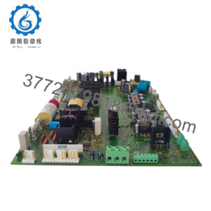
The Lam Research 810-069751-114 is a tool-specific Node Type 41 PCB assembly associated with Lam Research semiconductor manufacturing equipment. Current industrial inventory records identify the exact part number as a Node Type 41 board, including a Rev A listing.
Because public sources assign several conflicting functions to this part number, its exact electrical role should be established from the target tool’s BOM before replacement. Do not order this board solely from a description such as “RF interface” or “edge detector.”
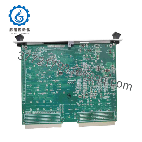
810-069751-114
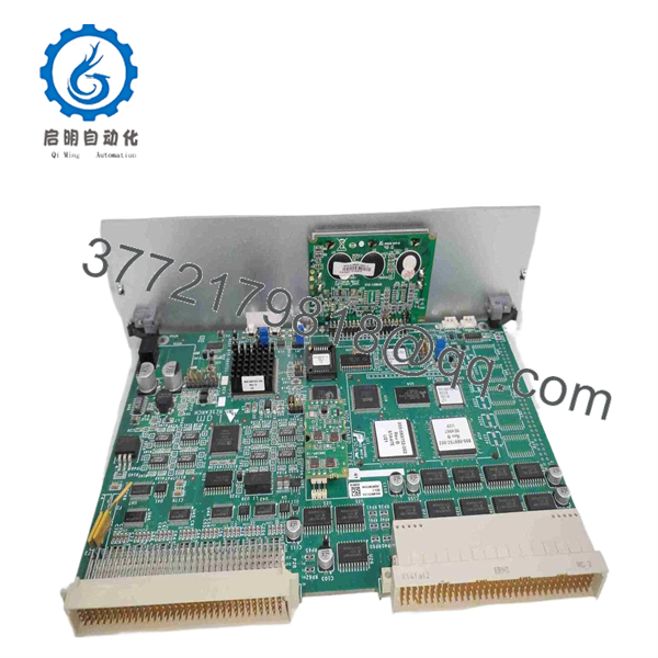
810-069751-114
Installation & Configuration Guide
Estimated replacement time: 30–60 minutes for an experienced semiconductor-equipment technician, excluding equipment qualification.
Stage 1: Pre-Installation Preparation
⚠️ Safety First
- Place the Lam Research tool in the approved maintenance state.
- Stop wafer processing and complete the equipment shutdown sequence.
- Apply electrical LOTO and isolate applicable pneumatic, vacuum, RF, and process-gas energy.
- Verify stored energy has been removed.
- Follow the fab’s ESD and contamination-control procedures.
- Confirm the cabinet/card cage is safe to access.
Tools Required
- ESD wrist strap
- Cleanroom gloves
- Precision screwdriver set
- Digital multimeter
- Connector labels
- Camera/smartphone
- Torque-controlled driver where specified
- Equipment configuration backup
Data Backup
Before removing the existing board:
- Photograph the complete installed board.
- Record 810-069751-114.
- Record the PCB revision.
- Photograph all connectors.
- Record the card-cage position.
- Photograph jumper and switch settings, if fitted.
- Record current tool alarms.
- Save the applicable tool configuration.
⚠️ The suffix matters. Do not replace a -114 board with another 810-069751 assembly simply because the PCB appears physically similar.
Stage 2: Removing the Old Module
- Confirm the tool is in its approved maintenance state.
- Verify electrical isolation.
- Photograph the board and cable arrangement.
- Label each connector.
- Disconnect connectors by the connector housing.
- Release the PCB mounting hardware.
- Pull the board straight out of its card position.
- Place the removed board in an ESD-safe bag.
- Inspect the card-cage connector and mating contacts.
Check for:
- Bent pins
- Oxidation
- Contamination
- Heat damage
- Loose connectors
- Cracked PCB material
- Damaged mounting hardware
Estimated time: 10–20 minutes.
Stage 3: Installing the New Module
- Verify the replacement label reads 810-069751-114.
- Confirm the PCB revision against the removed board.
- Compare the component layout.
- Compare every connector location.
- Wear ESD protection.
- Insert the board without forcing the backplane connector.
- Secure the board.
- Reconnect cables according to the photographs.
- Verify connector locks.
- Check grounding/bonding connections where applicable.
Configuration Clone — Critical
Before applying power:
- Compare all jumpers.
- Compare DIP switches, if fitted.
- Verify any address or node-selection settings.
- Confirm connector assignments.
- Verify the board occupies the same equipment position as the original.
Self-Checklist
- 810-069751-114 verified
- Revision verified
- Node Type 41 identification verified
- Correct card position confirmed
- Connector layout matched
- Jumpers/switches copied
- Cables secured
- ESD precautions maintained
Stage 4: Power-On & Testing
- Perform a complete visual inspection.
- Check for loose hardware and foreign objects.
- Restore equipment power according to the Lam Research procedure.
- Observe board status indicators, if fitted.
- Check host-controller diagnostics.
- Confirm the tool recognizes the installed node.
- Review node communication status.
- Test the affected I/O or subsystem through the approved service software.
- Verify applicable interlocks.
- Run the equipment’s dry-cycle/service test.
- Review diagnostic logs.
- Complete chamber/tool qualification before production release.
⚠️ Do not treat power-up as a functional test. A board can boot while an individual interface channel, feedback circuit, or synchronization function remains defective.
Frequently Asked Questions (FAQ)
1. What is Lam Research 810-069751-114?
The most defensible public identification is Lam Research Node Type 41 PCB Assembly. A current inventory listing specifically identifies a Rev A Node Board Type 41 with this exact part number.
2. Is 810-069751-114 an RF/DC interface board?
Some aftermarket sources describe it that way, associating the board with RF/DC control on Lam 2300-series equipment. However, another current inventory source identifies the same exact part number as a Node Type 41 board.
Because these descriptions conflict, I would not publish the RF/DC-interface designation as a confirmed OEM function without the target equipment documentation.
3. Is it an edge-detector board?
One secondary-market listing calls 810-069751-114 an edge detector junction board for 300 mm plasma-etch equipment. That conflicts with the Node Type 41 identification found elsewhere.
For procurement, use the exact part number plus the installed-tool model rather than relying on the generic functional title.
4. Can I substitute another 810-069751 board?
No automatic substitution should be assumed. Lam Research uses closely related numerical families for different boards. Verify the complete part number, revision, connector arrangement, tool model, and equipment BOM before installing an alternative.
5. Is 810-069751-114 obsolete?
It appears to be a legacy semiconductor-equipment spare, with current inventory primarily appearing through aftermarket and surplus channels. I did not find a public Lam Research lifecycle notice establishing an official EOL date.
6. What condition is available?
Current aftermarket listings show used and other inventory conditions. One current listing specifically identifies an 810-069751-114 Rev A unit as used.
For production-critical equipment, specify New Original/New Surplus or Refurbished Tested and request:
- Nameplate photographs
- PCB photographs
- Revision confirmation
- Functional test report
- Warranty terms
7. What should I verify before ordering?
At minimum, provide:
- 810-069751-114
- PCB revision
- Lam Research tool model
- Chamber/module designation
- Card-cage position
- Photographs of the installed board
- Connector photographs
- Required condition
- Required warranty
Given the contradictory public descriptions for this part, a photograph of the actual board is particularly valuable. It can help distinguish the physical assembly and revision from reseller catalog errors.