 WhatsApp: +86 16626708626
 Email:
 Phone: +86 16626708626
Description
Key Technical Specifications
| Parameter | Value |
| Bus Type | PCI |
| FPGA Chipset | Xilinx Virtex-II (XC2V1000) |
| Analog Input Channels | 8 Single-Ended / 16-Bit |
| Analog Output Channels | 8 Single-Ended / 16-Bit |
| Digital I/O Lines | 64 TTL/CMOS Lines |
| Maximum Sample Rate | 200 kS/s (Analog Inputs) |
| Operating Temperature | 0 to 55°C |
| Power Requirements | +5 VDC (2.5 A), +3.3 VDC (1.5 A) |
Product Introduction & Supply Chain Strategy
The National Instruments PCI-7813R is an advanced reconfigurable I/O (RIO) board powered by a user-programmable Xilinx Virtex-II FPGA. It enables engineers to design custom hardware timing, triggering, and closed-loop control algorithms directly on the board using LabVIEW FPGA, making it essential for high-speed simulation, hardware-in-the-loop (HIL) testing, and specialized industrial automation.
Securing this mature FPGA controller as a Brand New Surplus unit protects your capital investment and prevents catastrophic test bench downtime. Because this hardware platform is approaching end-of-life status through standard primary channels, holding verified OEM surplus stock on-site eliminates the severe performance risks and latent electrical faults common in second-hand or repaired boards.
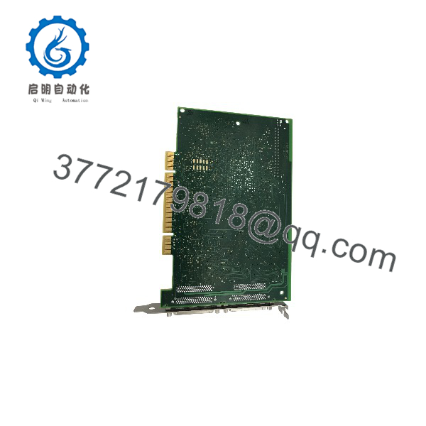
PCI-7813R
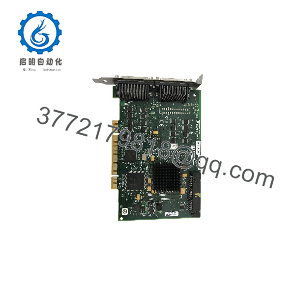
PCI-7813R
Installation & Configuration Guide
Stage 1: Pre-Installation (Prep & Safety)
- Perform complete lock-out/tag-out (LOTO) procedures on the host workstation or industrial chassis.
- Put on a grounded ESD wrist strap to protect static-sensitive CMOS FPGA structures and onboard memory chips.
- Back up your existing LabVIEW FPGA VI bitfile configurations and document all connected terminal blocks and cable maps.
Stage 2: Removal
- Disconnect all multi-pin shielded cables (such as SHC68-68-EPM) from the front brackets.
- Remove the retaining screw securing the PCI card bracket to the chassis frame.
- Extract the module smoothly along its slot axis to prevent bending backplane pins or straining adjacent components.
Stage 3: Installation (Clone & Seat)
- Confirm that no physical jumper configurations or daughterboard connections have shifted during transit.
- Align the gold-plated edge connector precisely with an open PCI slot and press down firmly until seated.
- Fasten the mounting bracket screw to ensure solid chassis grounding.
Stage 4: Power-On & Testing
- Restore system power and verify that the host operating system boots without device conflict errors.
- Open NI MAX (Measurement & Automation Explorer) and the NI-RIO driver interface to confirm device recognition.
- Download and execute a test bitfile to verify FPGA communication, clock generation, and I/O responsiveness before deploying to production.
Firmware/Software Versions & Upgrade Notes
- Recommended Driver: NI-RIO and NI-DAQmx driver suites matching your specific LabVIEW FPGA development environment (typically legacy v14.x or earlier for Virtex-II architectures).
- Compatibility Warning: Newer versions of LabVIEW and the NI-RIO driver may drop support for legacy Virtex-II generation targets. Always verify development toolkit compatibility before upgrading host software.
- Upgrade Risk: Compiling and flashing incompatible bitfiles to legacy hardware can cause bus lockups or execution errors. Keep your software build environment strictly version-locked to match installed hardware targets.
Frequently Asked Questions (FAQ)
Are these parts genuinely new, or are they refurbished?
This product is a Brand New Surplus unit. It has never been deployed in an active test cell, never undergone component-level repairs, and ships in original factory packaging.
Why is this priced lower than direct OEM list prices but higher than secondary-market refurbished units?
Our pricing reflects the strict sourcing and authentication required to secure genuine, factory-sealed surplus inventory globally. While it carries a modest premium over risky used alternatives, it completely eliminates the threat of premature FPGA failure and expensive project delays.
What is the obsolescence status of this module?
The PCI-7813R has reached mature EOL status as industrial computing shifts toward PCIe and PXI Express platforms. Maintaining a New Surplus buffer stock ensures continuous operation of your legacy test assets without emergency redesign costs.
What are the risks of using a refurbished alternative instead?
Refurbished FPGA boards frequently suffer from heat-stressed silicon, degraded decoupling capacitors, and intermittent solder micro-fractures. A subtle hardware failure inside the FPGA fabric can corrupt real-time control loops and trigger unsafe machine states.
What warranty is provided with this unit?
Every New Surplus PCI-7813R module is backed by our comprehensive 1-year replacement warranty, delivering long-term reliability and total peace of mind.