 WhatsApp: +86 16626708626
 Email:
 Phone: +86 16626708626
Description
Core Product Summary
The National Instruments PXI-5402 is a 3U, one-slot PXI waveform generator with a single 14-bit analog output channel. It generates standard sine, square, triangle, and ramp functions as well as user-defined waveforms, pseudorandom noise, and DC signals using direct digital synthesis.
The module provides up to 20 MHz sine or square output, up to 1 MHz triangle and ramp output, and up to 400 MS/s sampling for user-defined waveforms. Its BNC front panel includes the CH 0 analog output, REF IN clock input, and two bidirectional SYNC OUT/PFI connections. The PXI-5402 supports phase locking to an external reference or PXI_CLK10, PXI trigger lines, and NI-TClk synchronization with compatible modules.
Key Technical Specifications
| Attribute | Specification |
|---|---|
| Manufacturer | National Instruments (NI) |
| Model | PXI-5402 |
| Product type | PXI arbitrary function / waveform generator |
| Form factor | 3U, one-slot PXI/CompactPCI module |
| Output channels | 1 |
| DAC resolution | 14 bits |
| Analog output bandwidth | 20 MHz |
| Maximum sine frequency | 20 MHz |
| Maximum square frequency | 20 MHz |
| Maximum triangle frequency | 1 MHz |
| Maximum ramp frequency | 1 MHz |
| Maximum user-defined waveform frequency | 20 MHz, with interpolation set to 4 |
| Maximum sample rate | 400 MS/s for sine, square, and user-defined waveforms; 100 MS/s for triangle, ramp, and noise |
| User-defined waveform size | 16,384 samples |
| Frequency resolution | 0.355 µHz |
| Output impedance | Software-selectable 50 Ω or 75 Ω |
| Maximum output voltage | ±5 V (AC peak plus DC) |
| Amplitude range into 50 Ω | 5.64 mVpk-pk to 10 Vpk-pk |
| Amplitude range into high impedance | 11.28 mVpk-pk to 20 Vpk-pk |
| Output attenuation | 0 dB to 51 dB |
| Phase adjustment | −180° to +180° |
| Frequency-list steps | 1 to 58,235 steps |
| Frequency-list step duration | 1 ms to 21 s |
| Onboard frequency-list memory | 32 MB |
| PLL reference sources | REF IN, PXI_CLK10, or none |
| PLL reference frequency range | 5 MHz to 20 MHz in 1 MHz steps; default 10 MHz |
| Internal clock accuracy | ±25 ppm when PLL reference is set to none |
| PXI trigger lines | PXI_Trig<0..7> |
| Start-trigger modes | Single, continuous, stepped, and burst |
| Total power consumption | 17.6 W |
| Dimensions | 21.6 × 2.0 × 13.0 cm (8.5 × 0.8 × 5.1 in.) |
| Weight | 351 g (12.4 oz) |
| Operating temperature | 0 °C to 55 °C |
| Operating relative humidity | 10% to 90%, noncondensing |
| Storage temperature | −40 °C to 71 °C |
Engineering Selection Highlights
- The PXI-5402 provides one 14-bit output channel, so multi-channel stimulus requires multiple generator modules or a different multi-channel instrument.
- Its 20 MHz analog bandwidth and 20 MHz sine/square capability define the upper frequency range for standard function generation.
- The module supports 400 MS/s user-defined waveform sampling, but triangle, ramp, and noise generation are limited to 100 MS/s.
- The 16,384-sample user-defined waveform size is a key constraint when planning arbitrary waveform sequences or long test profiles.
- Software-selectable 50 Ω or 75 Ω output impedance and 0 dB to 51 dB attenuation allow the output path to be matched to different load and signal-level requirements.
- PLL synchronization accepts REF IN or PXI_CLK10, supporting frequency-accurate operation tied to an external reference or chassis clock.
- PXI trigger lines, two external trigger inputs, and NI-TClk support make the module suitable for coordinated multi-instrument test sequences.
Detailed Product Overview
The NI PXI-5402 is a single-channel, 14-bit PXI function and arbitrary waveform generator designed for modular test systems. It combines conventional DDS-based function generation with user-defined waveform playback, frequency-list operation, clock synchronization, and PXI triggering in a one-slot 3U module.
The analog output provides a maximum of ±5 V including both AC and DC components. Into a 50 Ω load, the amplitude range is 5.64 mVpk-pk to 10 Vpk-pk; into a high-impedance load, it is 11.28 mVpk-pk to 20 Vpk-pk. NI-FGEN compensates for a user-specified resistive load, and the output impedance can be configured as 50 Ω or 75 Ω. When the output is disabled, CH 0 is terminated to ground through a 1 W resistor equal to the selected output impedance.
Standard-function capability extends to 20 MHz for sine and square waves and 1 MHz for triangle and ramp waveforms. User-defined waveforms can reach 20 MHz when interpolation is set to 4, with a maximum sample rate of 400 MS/s. Noise generation is specified at up to 100 MS/s. The 16,384-sample waveform memory and 32 MB frequency-list memory define the practical limits for arbitrary waveform and frequency-sweep applications.
Timing flexibility is a central feature. The internal VCXO provides ±25 ppm frequency accuracy when no PLL reference is selected. For reference-locked operation, the module accepts a 5–20 MHz external reference through REF IN or uses PXI_CLK10; PLL lock time is typically 70 ms and no more than 200 ms. The module can also export its sample clock or PLL reference through SYNC OUT/PFI 0, PFI 1, or PXI_Trig<0..6>.
Triggering supports immediate, software, external, PXI trigger-line, and PXI Star Trigger sources. Available modes are single, continuous, stepped, and burst, with rising-edge, falling-edge, high-level, and low-level detection. The minimum external trigger pulse width is 25 ns. These options allow waveform generation to be coordinated with other instruments or with events in the device under test.
The module includes onboard self-calibration using a 24-bit ADC and precision voltage reference. Software-initiated self-calibration adjusts gain, offset, and square-wave duty cycle and takes approximately 105 seconds. External calibration addresses the VCXO, voltage reference, self-calibration ADC, flatness, gain, and offset; published specifications are valid within two years of external calibration. A 15-minute warm-up period applies.
The PXI-5402 is intended for indoor use in industrial locations and operates from 0 °C to 55 °C at 10% to 90% noncondensing relative humidity. It is designed to meet IEC 61010-1, EN 61010-1, UL 61010-1, and CSA C22.2 No. 61010-1 safety-standard requirements, and it complies with the listed EMC standards for measurement, control, and laboratory-use equipment.
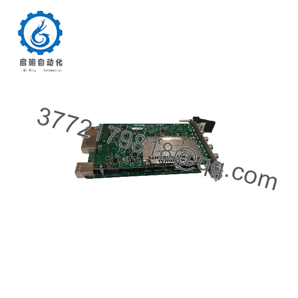
PXI-5402
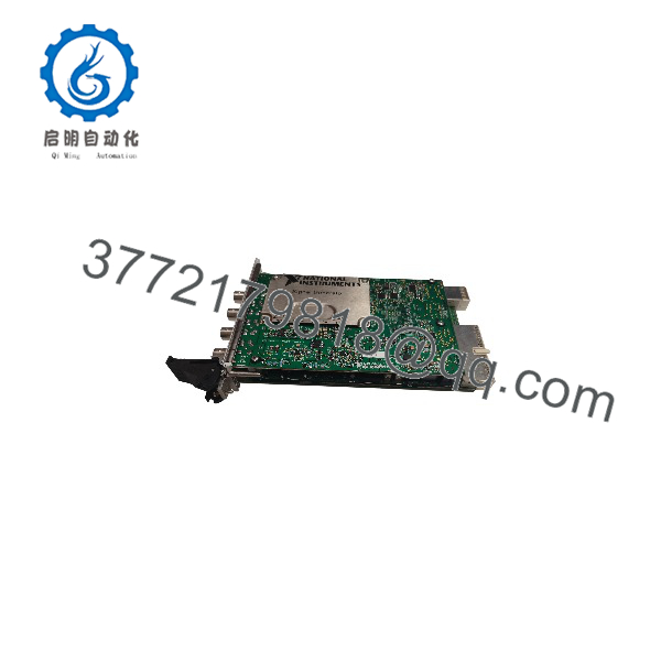
PXI-5402
System Compatibility & Integration Requirements
| Item / Dependency | Verified Compatibility or Requirement | Practical Note |
|---|---|---|
| Chassis format | 3U PXI or CompactPCI chassis | The module occupies one 3U peripheral slot. |
| PXI timing | PXI_CLK10 and PXI_Trig<0..7> | PXI_CLK10 can serve as the PLL reference; PXI trigger lines support start triggering and signal routing. |
| External reference | REF IN BNC input, 5–20 MHz in 1 MHz steps | The reference source must be accurate to ±50 ppm to guarantee PLL locking. |
| External triggering | SYNC OUT/PFI 0 and PFI 1 BNC connectors | Both connectors accept external start or step triggers and can output timing or event signals. |
| Software | NI-FGEN | NI-FGEN programs and controls the module; the ACCESS LED turns green when the device is ready for NI-FGEN programming. |
| Synchronization | NI-TClk | NI-TClk aligns sample clocks across compatible SMC-based modules; published skew figures apply to identical modules in one PXI-1042 chassis under the stated configuration. |
| Cabling | Shielded cables and accessories | NI specifies shielded cables and accessories for the stated EMC performance. |
| Cooling | Forced-air PXI chassis cooling | The module requires forced-air cooling; an internal over-temperature condition causes a thermal shutdown and requires correction before reset. |
Dimensions, Mounting & Connection Notes
The PXI-5402 is a 3U, one-slot PXI/CompactPCI module measuring 21.6 cm high, 2.0 cm wide, and 13.0 cm deep. It weighs 351 g.
The front panel provides four BNC connectors:
- CH 0 — analog waveform output.
- REF IN — external PLL reference-clock input; 50 Ω impedance, AC coupled.
- SYNC OUT/PFI 0 — bidirectional TTL-compatible timing, trigger, and event connection.
- PFI 1 — bidirectional TTL-compatible timing, trigger, and event connection.
The front panel also includes ACCESS and ACTIVE status LEDs. ACCESS indicates power, access, and readiness status; ACTIVE indicates idle, armed, generating, or error states. A red ACTIVE LED can indicate an unlocked PLL or an internal over-temperature shutdown.
The module draws 1.4 A at +3.3 VDC, 0.11 A at +12 VDC, 0.01 A at −12 VDC, and a frequency- and amplitude-dependent current at +5 VDC. Total power consumption is 17.6 W.
Applications & System Role
The PXI-5402 serves as the stimulus source in a PXI-based automated test system. It produces controlled analog signals for device characterization, functional testing, filter and amplifier response testing, sensor excitation, communications-related signal generation, and other applications requiring repeatable voltage waveforms.
Its direct digital synthesis architecture supports standard functions as well as user-defined waveforms. The 32 MB frequency-list memory, frequency-list mode, and stepped triggering support frequency sweeps and stepped-frequency test sequences without relying solely on continuous host-software control.
In a multi-module PXI system, the module can use PXI_CLK10, external REF IN, PXI trigger lines, front-panel PFI connections, and NI-TClk to coordinate generation with digitizers, switches, digital instruments, or other signal generators. This makes it appropriate for synchronized stimulus-and-response test architectures.
FAQ
What is the NI PXI-5402?
The NI PXI-5402 is a 3U, one-slot PXI waveform generator with one 14-bit analog output channel and 20 MHz analog bandwidth.
What waveforms can the PXI-5402 generate?
It generates sine, square, triangle, ramp-up, ramp-down, user-defined, pseudorandom-noise, and DC signals.
What is the maximum output frequency?
The maximum sine and square frequency is 20 MHz. Triangle and ramp output is limited to 1 MHz.
What is the maximum sample rate?
The maximum sample rate is 400 MS/s for sine, square, and user-defined waveforms. Triangle, ramp, and noise generation is limited to 100 MS/s.
What output amplitude does the PXI-5402 provide?
Into a 50 Ω load, the amplitude range is 5.64 mVpk-pk to 10 Vpk-pk. Into a high-impedance load, it is 11.28 mVpk-pk to 20 Vpk-pk. The absolute maximum output voltage is ±5 V including AC and DC components.
Which chassis slots and modules does it require?
It requires one 3U PXI or CompactPCI peripheral slot and forced-air chassis cooling.
How is the PXI-5402 synchronized?
It can phase-lock to an external reference through REF IN or to PXI_CLK10. It also supports PXI trigger lines, front-panel PFI triggering, and NI-TClk synchronization.
What software controls the PXI-5402?
NI-FGEN is the NI instrument driver used to program and control the module.