 WhatsApp: +86 16626708626
 Email:
  Phone: +86 16626708626
Description
Key Technical Specifications
| Parameter | Value |
|---|---|
| Manufacturer | LAM Research |
| Part Number | 810-810202-013 |
| Product Type | PCB Assembly |
| Application | LAM semiconductor processing equipment |
| Equipment Function | Equipment-specific control/interface function |
| Board Revision | Verify physical PCB marking |
| Communication Interface | Verify against applicable LAM equipment documentation |
| Input/Output Configuration | Not reliably established from the available public identification |
| Supply Voltage | Verify from OEM equipment documentation |
| Connector Configuration | Verify from physical board and equipment wiring documentation |
| Firmware | Verify, if applicable |
| Mechanical Dimensions | Verify against OEM drawing |
| Operating Temperature | Verify against equipment-level specification |
| Replacement Compatibility | Must be matched to the target LAM tool/configuration |
Procurement note: I would not attach unverified voltage, I/O-channel, communication, or firmware specifications to 810-810202-013 without the applicable LAM documentation or a clear photograph of the actual board. For legacy semiconductor equipment, the assembly number alone is not always enough to establish a safe substitute.
Product Introduction
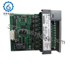
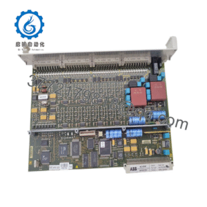
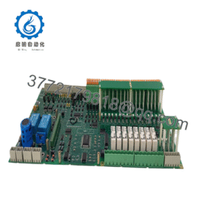
The LAM Research 810-810202-013 is an equipment-specific PCB assembly used within LAM Research semiconductor processing equipment. Its exact circuit function, connector assignment, and electrical characteristics should be confirmed against the target tool configuration and the physical board revision.
For replacement work, match the complete 810-810202-013 number rather than purchasing by a generic description such as “LAM PCB.” Compare board revision, connector layout, labels, and installed configuration before installation.
Installation & Configuration Guide
Stage 1: Pre-Installation Preparation — 10–15 Minutes
⚠️ Safety First: Put the LAM tool into its approved maintenance state. Complete site lockout/tagout and verify the required electrical and process hazards have been controlled before accessing the PCB.
Tools Required
- ESD wrist strap
- ESD-safe work surface
- Digital multimeter
- Appropriate screwdriver set
- Connector labels
- Smartphone/camera
- Applicable LAM service documentation
Data Backup
Before removing the existing board:
- Record 810-810202-013 from the board label.
- Photograph the complete PCB.
- Photograph all connectors and cable routing.
- Record the PCB revision.
- Photograph switches, jumpers, and configuration links.
- Record the LAM tool model and relevant controller configuration.
- Keep the removed board until commissioning is complete.
Stage 2: Removing the Old Module — 5–10 Minutes
- Place the equipment in its approved maintenance state.
- Isolate power according to the site procedure.
- Verify the de-energized condition.
- Attach ESD protection.
- Photograph the installed board before touching the wiring.
- Label each cable and connector.
- Disconnect connectors carefully.
- Remove retaining screws or mounting hardware.
- Withdraw the PCB without twisting it.
- Inspect the mating connectors for bent contacts, contamination, or mechanical damage.
⚠️ Do not pull on cable conductors. Use the connector body or approved extraction mechanism.
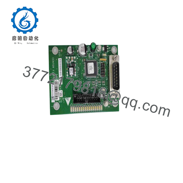
810-810202-013
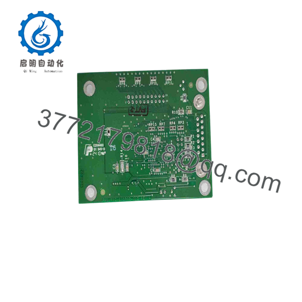
810-810202-013
Stage 3: Installing the New 810-810202-013 — 10 Minutes
1. Verify the Replacement
Confirm:
- 810-810202-013 part number
- PCB revision
- Connector arrangement
- Mounting-hole pattern
- Board markings
- Component population
2. Compare With the Original
Place the two boards side by side and check:
- Connector positions
- Connector labels
- Jumpers
- Switches
- PCB revision
- Cable interfaces
- Mounting hardware
- Daughter-board or ribbon-cable interfaces
3. Install the PCB
- Align the PCB with its guides or mounting points.
- Seat it without excessive force.
- Secure the retaining hardware.
- Reconnect each cable using the photographs and labels.
- Confirm every connector is fully seated.
Self-Checklist
- Exact 810-810202-013 confirmed
- PCB revision checked
- Connector layout matched
- Cable labels verified
- Configuration settings copied
- Mounting hardware secured
- Connectors fully seated
Stage 4: Power-On & Testing — 10–20 Minutes
Pre-Power Check
Inspect:
- PCB surface
- Connectors
- Cable routing
- Mounting hardware
- Grounding connections
- Signs of contamination or component damage
Verify applicable supply rails using the LAM equipment documentation.
Power-Up
- Restore power following the approved LAM sequence.
- Observe system and board indicators.
- Allow the controller to complete initialization.
- Check equipment diagnostics.
- Verify the functions associated with the replaced board.
- Check connected interfaces.
- Run the approved equipment functional test.
- Monitor the system before returning the tool to production.
Troubleshooting
No board response:
Check board seating, supply voltage, grounding, connectors, and the exact PCB revision.
Controller reports an equipment fault:
Compare the replacement configuration with the original board and verify that all connectors are installed in their original positions.
Intermittent operation:
Inspect connectors, cable strain, grounding, and board seating before replacing additional components.
System will not initialize:
Stop repeated power cycling. Confirm the exact part number, revision, tool compatibility, and applicable LAM service procedure.
Frequently Asked Questions (FAQ)
What is LAM 810-810202-013?
It is a LAM Research PCB assembly associated with semiconductor processing equipment. The precise circuit function should be verified against the target LAM tool and physical board documentation before procurement.
Is 810-810202-013 a PLC or I/O module?
It should not automatically be classified as a conventional PLC CPU or standard I/O module. The available identification supports treating it as an equipment-specific PCB assembly. The exact electrical function requires LAM equipment documentation or physical-board verification.
Can I replace 810-810202-013 with another LAM PCB?
Not without compatibility verification. Similar-looking LAM boards can have different connector assignments, revisions, or equipment functions. Match the complete part number and compare the original board before substitution.
Is 810-810202-013 obsolete?
A definitive OEM lifecycle status has not been established here. Because this is a legacy semiconductor-equipment spare, verify current stock, production status, and available replacement options before planning a long-term maintenance strategy.
Can this PCB be hot-swapped?
Do not assume so. Unless the applicable LAM equipment documentation explicitly identifies 810-810202-013 as hot-swappable, perform replacement with the equipment isolated according to the approved maintenance procedure.
Will replacing the PCB erase my equipment configuration?
That depends on where the configuration is stored in the particular LAM system. Before removal, document all accessible switches, jumpers, addresses, and configuration settings. Do not assume the replacement board will automatically inherit the old configuration.
What information should I provide when ordering?
Provide:
- LAM 810-810202-013
- LAM equipment/tool model
- PCB revision
- Photograph of the board label
- Photographs of connectors
- Required quantity
- Required condition
- Required delivery date
For this part, a clear photograph of the actual PCB label and connector side would materially improve identification, especially if you need the exact board function and compatibility checked.