 WhatsApp: +86 16626708626
 Email:
 Phone: +86 16626708626
Description
Core Product Summary
The National Instruments PXI-7852R is a 3U PXI R Series Multifunction Reconfigurable I/O module built around a user-programmable Xilinx Virtex-5 LX50 FPGA. It combines eight 16-bit analog inputs, eight 16-bit analog outputs, and 96 bidirectional digital I/O lines in a single PXI module.
Analog inputs support simultaneous sampling at up to 750 kS/s per channel with a fixed ±10 V range. Analog outputs support up to 1 MS/s per channel. The FPGA controls the analog and digital I/O resources, allowing custom timing, triggering, processing, counting, and control logic to be implemented with the LabVIEW FPGA Module. The module uses a 68-pin female VHDCI connector and supports PXI_CLK10 synchronization, PXI trigger lines, and the PXI star trigger.
Key Technical Specifications
| Attribute | Specification |
|---|---|
| Manufacturer | National Instruments (NI) |
| Model | PXI-7852R |
| Product type | R Series Multifunction Reconfigurable I/O module |
| Form factor | 3U PXI module |
| FPGA | Xilinx Virtex-5 LX50 |
| Analog-input channels | 8 |
| Analog-input resolution | 16 bits |
| Analog-input sample rate | Up to 750 kS/s per channel |
| Analog-input sampling | Simultaneous or independently timed per channel |
| Analog-input range | Fixed ±10 V |
| Analog-input data format | Two’s complement |
| Analog-output channels | 8 |
| Analog-output resolution | 16 bits |
| Analog-output update rate | Up to 1 MS/s per channel |
| Digital I/O | 96 bidirectional lines |
| Digital I/O configuration | Individually configurable as input or output |
| Digital I/O rate | Up to 40 MHz |
| I/O connector | 68-pin female VHDCI |
| PXI timing | PXI_CLK10, PXI_Trig<0..7>, PXI star trigger |
| FPGA synchronization | FPGA clock can be phase-locked to PXI_CLK10 |
| Onboard storage | Flash memory for FPGA startup VI |
| Software development | LabVIEW FPGA Module |
| Host communication | FPGA Interface functions |
| Real-time control | LabVIEW Real-Time Module |
| Device temperature reporting | Onboard sensor, 0.25 °C increments |
| Part number | 780340-01 |
Engineering Selection Highlights
- The PXI-7852R provides eight independent 16-bit analog inputs, each capable of up to 750 kS/s, allowing simultaneous or individually timed acquisition.
- Its eight 16-bit analog outputs update at up to 1 MS/s per channel, supporting coordinated stimulus, control, and waveform generation.
- The 96 bidirectional digital I/O lines can be configured individually as inputs or outputs and used for counters, timers, or custom FPGA logic.
- The Virtex-5 LX50 FPGA defines the available logic capacity for user-defined timing, processing, control loops, and I/O behavior.
- The module’s fixed ±10 V analog-input range should be checked against signal levels; external signal conditioning is required for other ranges.
- PXI_CLK10, eight PXI trigger lines, and the PXI star trigger support synchronization with other PXI instruments.
- The 68-pin female VHDCI connector requires compatible R Series cabling and a connector block or custom cable for field wiring.
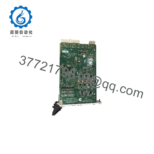
PXI-7852R
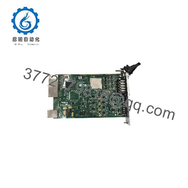
PXI-7852R
System Compatibility & Integration Requirements
| Item / Dependency | Verified Compatibility or Requirement | Practical Note |
|---|---|---|
| Chassis format | 3U PXI chassis | The module is a PXI R Series Multifunction RIO device. |
| CompactPCI operation | Compatible with PICMG CompactPCI 2.0 R3.0 core specification | PXI-specific functions such as the RTSI/PXI trigger bus are available only in a PXI chassis. |
| Analog inputs | AI<0..7>, fixed ±10 V range | Channels can be sampled simultaneously or at different rates. |
| Analog outputs | AO<0..7> | Accessed through FPGA I/O Nodes configured for writing. |
| Digital I/O | 96 lines, configurable as inputs or outputs | Digital outputs must be written as either a port or a line, not both. |
| FPGA development | LabVIEW FPGA Module | Required to create or modify FPGA VIs for the module. |
| Existing FPGA VIs | LabVIEW or LabVIEW Real-Time Module | Host VIs can control an existing FPGA VI without the FPGA Module. |
| Startup configuration | Flash memory | A startup VI can be stored in Flash and loaded automatically at power-up. |
| PXI synchronization | PXI_CLK10, PXI_Trig<0..7>, PXI_Star | The FPGA clock can be phase-locked to PXI_CLK10 using RIO Device Setup. |
| Cabling | SHC68-68-RDIO, SH68-C68-S, or SHC68-NT-S cable options | NI recommends shielded cabling for signal integrity and noise immunity. |
| Connector accessory | NI SCB-68 terminal block | Compatible cable/accessory combinations are documented for R Series connectivity. |
Dimensions, Mounting & Connection Notes
The PXI-7852R is a 3U PXI module with a 68-pin female VHDCI front-panel connector. Its listed weight is 0.41 kg.
The module provides three VHDCI-based I/O connector groups in the R Series 785xR architecture: Connector 0 is the mixed analog/digital I/O connector, while Connectors 1 and 2 provide digital I/O. The analog-input channels are designated AI<0..7>, analog outputs AO<0..7>, and digital lines are organized by connector and port.
The module includes Flash memory for storing a startup FPGA VI. The FPGA VI is not retained when power is removed, so it must be reloaded from Flash or over the bus interface after power-up. The onboard device-temperature sensor reports temperature in 0.25 °C increments.
For field connections, NI documents the SHC68-68-RDIO shielded cable for Connectors 0 through 2, the SH68-C68-S basic shielded cable, and the SHC68-NT-S unterminated custom-cable option. The SHC68-68-RDIO can connect to an NI SCB-68 terminal block.
Detailed Product Overview
The NI PXI-7852R is a member of NI’s R Series Multifunction RIO family. Its defining feature is the user-programmable Virtex-5 LX50 FPGA, which controls the module’s fixed analog and digital I/O resources. Rather than providing only fixed-function DAQ behavior, the module allows users to define timing, triggering, processing, and I/O logic in LabVIEW FPGA and deploy that logic directly to the hardware.
The analog-input section provides eight independent 16-bit channels with a fixed ±10 V input range. Channels can be sampled simultaneously or at different rates, and each channel supports up to 750 kS/s. The converters return data in two’s-complement format. The analog-input architecture uses instrumentation amplifiers, input multiplexing, and calibration circuitry, with software-configurable input modes.
The analog-output section provides eight independent 16-bit channels with an update rate of up to 1 MS/s per channel. These outputs are accessed through FPGA I/O Nodes configured for writing. Together, the analog-input and analog-output resources support closed-loop applications where measurement, computation, and actuation occur within the same FPGA-controlled module.
The digital section provides 96 bidirectional lines, individually configurable as inputs or outputs. These lines can be used for general-purpose digital I/O, counters, timers, or custom logic. NI documents digital operation at rates up to 40 MHz. The FPGA I/O interface supports line-level and port-level access, with the restriction that a digital output must be written as either a port or a line.
Timing and synchronization are implemented through the PXI backplane. The module can access PXI_CLK10 for multi-module synchronization, eight PXI trigger lines, and the PXI star trigger. The FPGA clock can be phase-locked to PXI_CLK10 through the RIO Device Setup utility. NI notes that writing to the PXI star-trigger channel while the module is installed in PXI slot 2 can affect 10 MHz clock accuracy and cause a PXI system malfunction.
Software development requires the LabVIEW FPGA Module to create or modify FPGA VIs. Host applications can use LabVIEW or the LabVIEW Real-Time Module to communicate with an already compiled FPGA VI through FPGA Interface functions. The module’s Flash memory can store a startup VI, allowing the FPGA application to begin execution shortly after power-up rather than waiting for a host computer to load it.
The PXI-7852R is part number 780340-01 and is intended for PXI systems requiring a combination of FPGA-defined behavior, multichannel analog I/O, and high-density digital I/O. Its exact suitability depends on the compiled FPGA design, the available LX50 logic resources, the required I/O timing, and the electrical characteristics of the connected signals.
Applications & System Role
The PXI-7852R functions as a reconfigurable measurement, control, and timing module within a PXI system. Its FPGA sits between the PXI bus interface and the fixed analog and digital I/O resources, allowing the module to implement application-specific acquisition, generation, logic, and synchronization behavior.
Typical system roles include closed-loop control, hardware-in-the-loop simulation, custom event counting, encoder processing, digital protocol emulation, custom triggering, and coordinated analog/digital test sequences. NI describes R Series devices as suitable for applications requiring real-time processing, datalogging, timing, triggering, and I/O logic.
The module can operate as a single-point analog-input, analog-output, and digital-I/O complement to a LabVIEW Real-Time system. It can also execute FPGA logic independently of host software, provided the required FPGA VI has been compiled and deployed to the module or stored in its Flash memory.
FAQ
What is the NI PXI-7852R?
The NI PXI-7852R is a 3U PXI R Series Multifunction Reconfigurable I/O module with a Virtex-5 LX50 FPGA, eight analog inputs, eight analog outputs, and 96 digital I/O lines.
Which FPGA does the PXI-7852R use?
It uses a Xilinx Virtex-5 LX50 FPGA.
What are the analog-input capabilities?
It has eight 16-bit analog-input channels with a fixed ±10 V range and a maximum sample rate of 750 kS/s per channel.
What are the analog-output capabilities?
It has eight 16-bit analog-output channels with an update rate of up to 1 MS/s per channel.
How many digital I/O lines does it provide?
It provides 96 bidirectional digital I/O lines, individually configurable as inputs or outputs.
What software is required to program the FPGA?
The LabVIEW FPGA Module is required to create or modify FPGA VIs for the PXI-7852R.
Can the PXI-7852R synchronize with other PXI modules?
Yes. It supports PXI_CLK10, PXI_Trig<0..7>, and the PXI star trigger. Its FPGA clock can be phase-locked to PXI_CLK10.
What connector does the PXI-7852R use?
It uses a 68-pin female VHDCI front-panel connector.